


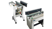


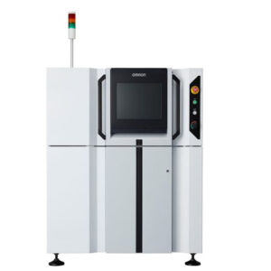
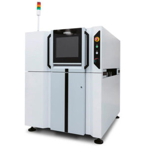
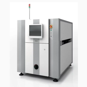
AOI / SPI Machines
AOI (Automated Optical Inspection) and SPI (Solder Paste Inspection) are essential systems in PCB (Printed Circuit Board) manufacturing lines used for quality control and ensuring the accuracy of assembly and soldering processes.
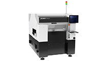
AOI (Automated Optical Inspection)
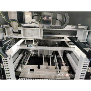
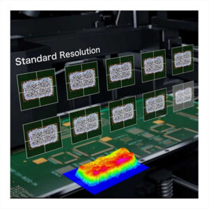
AOI is an inspection system that uses high-resolution cameras and specialized lighting to examine the quality of PCB assembly. It is typically used after SMD component placement and after reflow or wave soldering to detect assembly defects.
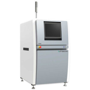
SPI (Solder Paste Inspection)
SPI is a device used to inspect the distribution, thickness, and uniformity of solder paste after it has been printed onto the PCB. The quality of solder paste directly impacts the success of the soldering process, making early inspection essential.
Features and Functionality of AOI
Automated visual inspection: The system captures images of the PCB and compares them with a reference to identify defects.
Detectable defects include:
- Missing components
- Misaligned components
- Solder bridges
- Cold solder joints
- Incorrect polarity of components
Uses image processing algorithms and AI to improve inspection accuracy.
Configurable and programmable according to PCB and component types.
Features and Functionality of SPI
3D Inspection: Uses laser sensors and specialized cameras to precisely measure the volume of solder paste.
Detectable defects include:
- Insufficient or excessive solder paste
- Misaligned solder paste
- Smeared solder paste
- Uneven distribution on pads
Uses image processing algorithms for fast and accurate defect detection.
Provides feedback to optimize solder paste printer settings.
Differences Between AOI and SPI and Their Roles in PCB Manufacturing
| Feature | AOI (Automated Optical Inspection) | SPI (Solder Paste Inspection) |
|---|---|---|
| Inspection Timing | After component placement and soldering | After solder paste printing, before placement |
| Purpose | Checks assembly and soldering accuracy | Ensures solder paste quality |
| Output Data | 2D and 3D images, defect reports | Solder paste thickness and distribution map |
| Detectable Defects | Missing components, misalignment, cold solder, solder bridges | Insufficient or excessive solder paste, misalignment |
| Impact on Production | Ensures final product quality control | Improves the soldering process by preventing defects |

